Come funziona una fabbrica di chip e quanta energia assorbe?
Quanta energia e acqua consuma una gigafab, quanto è pulita l'aria e come lavora l'EUV: dati NIST, ASML e TSMC, ognuno datato al suo anno di riferimento.
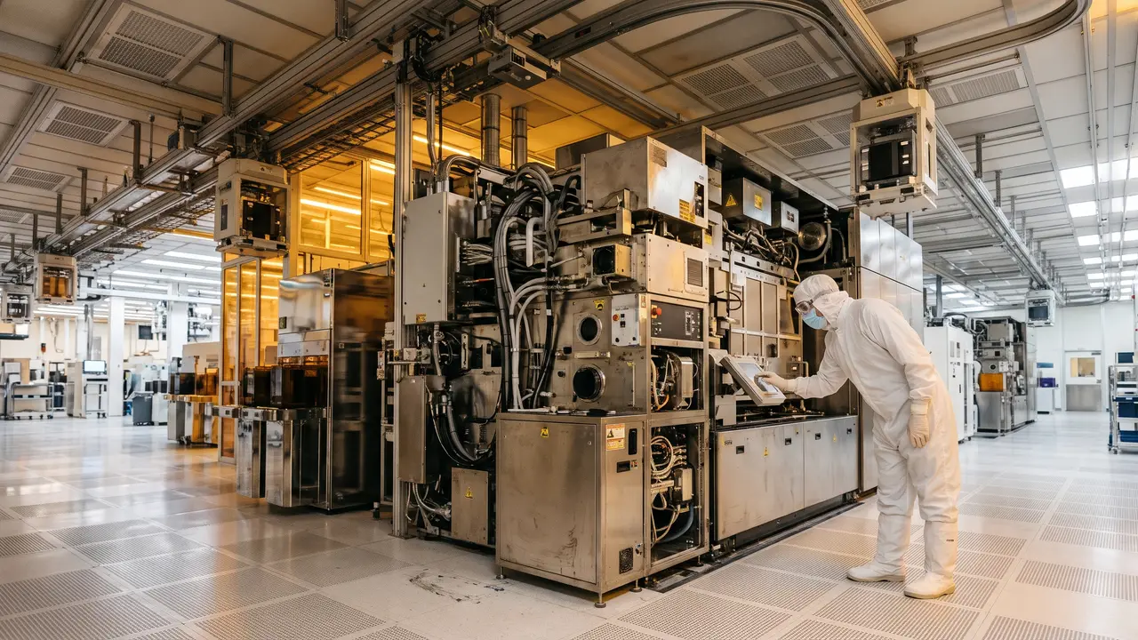
Le fab di semiconduttori lavorano spesso a livello ISO 7 o 5; il livello 1 è molto raro.
- Livello tipico delle fab
- ISO 7 o 5
- Il livello ISO 1 è molto raro negli impianti di semiconduttori[1]
In questo articolo
Salta a una sezione
Elettricità: dove finisce l'energia di una fab
- 1999 (EPRI): studio dei consumi in 14 fab[7]; media di 7,45 kWh per pollice quadrato (1,15 kWh/cm²) di wafer processato[8]; strumenti di processo con oltre il 40% dell'elettricità usata dalle fab[9].
- 2019 (TSMC): scaldabagni a ricircolo per la pulizia dei wafer, con l'acqua calda sprecata ridotta dell'80%[10]; 29 scaldabagni a ricircolo hanno risparmiato in totale 14 milioni di kWh (dato di novembre 2019)[11].
- 2020 (Intel): oltre 2.000 progetti di risparmio energetico in un decennio, con 4,5 milioni di MWh risparmiati secondo la dichiarazione dell'azienda[12].
Litografia EUV: stagno, laser a CO2 e una resa del 5-6%
5–6%
Acqua ultrapura: quanta ne serve e quanta si recupera
Camera bianca: livelli ISO 7 e 5, non ISO 1
Vibrazioni e costi: pali nella roccia, molle e miliardi
Da leggere · Computing e IA
Come fa la luce a superare l'oceano nei cavi sottomarini
Domande frequenti
Come funziona una fabbrica di chip in termini di energia e acqua?
Una fabbrica di chip lavora in camera bianca ISO 1?
Quanta luce EUV produce davvero una sorgente di una fabbrica di chip?
Che cos'è l'acqua ultrapura e quanta se ne ricicla in una fabbrica di chip?
Quanto costa costruire una fabbrica di chip?
Fonti
52 riferimenti Mostra Nascondi
- Wikipedia, Cleanroom (si apre in una nuova scheda)
«Semiconductor facilities often get by with level 7 or 5, while level 1 facilities are exceedingly rare.»
- NIST, Final PEA for Modernization and Expansion of Semiconductor Fabs (si apre in una nuova scheda)
«Of 29 fabs (the largest sample size available), the median energy usage in 2021 was approximately 2.74 million megawatt-hours (MWh) of power»
- NIST, Final PEA for Modernization and Expansion of Semiconductor Fabs (si apre in una nuova scheda)
«In 2021, the median ultra-pure water (UPW) usage among 29 fabs was approximately 4.25 billion gallons»
- NIST, Final PEA for Modernization and Expansion of Semiconductor Fabs (si apre in una nuova scheda)
«Lithography, etching, and deposition tend to be the most energy intensive process steps.»
- NIST, Final PEA for Modernization and Expansion of Semiconductor Fabs (si apre in una nuova scheda)
«Cleanrooms require energy for recirculation air flow and temperature and humidity control to meet contamination control requirements.»
- Wikipedia, Semiconductor fabrication plant (si apre in una nuova scheda)
«Very high consumption of electricity, heat, water, and cooling, with power needs in the terawatt-hour range per year.»
- EPRI, TR-113499 (si apre in una nuova scheda)
«Energy consumption levels were studied in 14 fabs»
- EPRI, TR-113499 (si apre in una nuova scheda)
«On average, the fabs in this study consumed 7.45 kWh/inch 2 (1.15 kWh/cm 2) of wafer processed»
- EPRI, TR-113499 (si apre in una nuova scheda)
«which consumed over 40% of the electrical energy used by the fabs»
- TSMC ESG (si apre in una nuova scheda)
«successfully reduced waste hot water by 80%»
- TSMC ESG (si apre in una nuova scheda)
«saving a total of 14M kWh of electricity»
- NIST, Final PEA for Modernization and Expansion of Semiconductor Fabs (si apre in una nuova scheda)
«Intel has completed more than 2,000 energy conservation projects in the last decade, saving 4.5 million MWh (Intel, 2020)»
- NIST, Final PEA for Modernization and Expansion of Semiconductor Fabs (si apre in una nuova scheda)
«onsite electricity generation among semiconductor fabrication facilities is primarily fossil fuel combustion (12 percent of total energy usage)»
- Wikipedia, Extreme ultraviolet lithography (si apre in una nuova scheda)
«Laser-produced plasma, or LPP, is the dominant light-source architecture used in commercial high-volume manufacturing (HVM) EUV lithography.»
- Wikipedia, Extreme ultraviolet lithography (si apre in una nuova scheda)
«The source operates at a repetition rate of ~50 kHz and conversion efficiency of ~5–6%.»
- Wikipedia, Extreme ultraviolet lithography (si apre in una nuova scheda)
«ejects ~25 μm diameter molten tin droplets at ~70 m/s through a vacuum chamber»
- Wikipedia, Extreme ultraviolet lithography (si apre in una nuova scheda)
«A dual-pulse carbon dioxide(CO2) laser system»
- Wikipedia, Extreme ultraviolet lithography (si apre in una nuova scheda)
«Since the mirrors absorb 96% of the EUV light»
- Wikipedia, Extreme ultraviolet lithography (si apre in una nuova scheda)
«which require the costly collector mirror to be replaced every year»
- Wikipedia, Extreme ultraviolet lithography (si apre in una nuova scheda)
«Current-generation LPP sources deliver approximately 250 W of in-band EUV power at intermediate focus»
- Wikipedia, Extreme ultraviolet lithography (si apre in una nuova scheda)
«to get 200 watts at intermediate focus for 100 wafers per hour, one would require 1 megawatt of input power»
- ASML, EUV lithography systems (si apre in una nuova scheda)
«The technology, which is unique to ASML, prints microchips using light with a wavelength of just 13.5 nm»
- ASML, EUV lithography systems (si apre in una nuova scheda)
«ASML invested more than €6 billion in EUV R&D over 17 years.»
- ASML, EUV lithography systems (si apre in una nuova scheda)
«We acquired Cymer – a company specialized in light source technology – to accelerate EUV source development.»
- ASML, 5 things you should know about High NA EUV (si apre in una nuova scheda)
«After a decade of R&D, ASML shipped the first modules of the first High NA EUV lithography system to Intel in December 2023.»
- ASML, 5 things you should know about High NA EUV (si apre in una nuova scheda)
«can print more than 185 wafers per hour»
- Wikipedia, Ultrapure water (si apre in una nuova scheda)
«Absolutely pure water has a conductivity of 0.05501 μS/cm and a resistivity of 18.18 MΩ⋅cm at 25 °C»
- Wikipedia, Ultrapure water (si apre in una nuova scheda)
«Resistivity is highly sensitive to contamination by ions»
- Wikipedia, Ultrapure water (si apre in una nuova scheda)
«Water purity requirements of the semiconductor industry are generally the most stringent to prevent circuit faults at the nanometer scale.»
- ASTM D5127 (si apre in una nuova scheda)
«Seven classifications of water are described, including water for line widths as low as 0.032 μm.»
- ASTM D5127 (si apre in una nuova scheda)
«High-purity water is required to prevent contamination of products during manufacture, since contamination can lead to an unacceptable, low yield of electronic devices.»
- Wikipedia, Ultrapure water (si apre in una nuova scheda)
«advanced fabrication plants consuming several million gallons of UPW per day»
- NIST, Final PEA for Modernization and Expansion of Semiconductor Fabs (si apre in una nuova scheda)
«abatement technologies to remove hazardous gases from SME (20 percent)»
- NIST, Final PEA for Modernization and Expansion of Semiconductor Fabs (si apre in una nuova scheda)
«UPW treatment losses (9 percent)»
- Wikipedia, Ultrapure water (si apre in una nuova scheda)
«some manufacturers have begun using reclaimed municipal or industrial wastewater as raw feedstock for UPW production»
- Wikipedia, Ultrapure water (si apre in una nuova scheda)
«Some systems recycle used UPW water back into their UPW filtration system as this water is often cleaner than original sources.»
- TSMC, Annual Report (si apre in una nuova scheda)
«The cumulative supply use of reclaimed water exceeded 67 thousand cubic meters per day»
- TSMC, Annual Report (si apre in una nuova scheda)
«This reduced city water usage by 31%»
- Taiwan Insight, Water nexus: can semiconductors and sustainability coexist in Taiwan (si apre in una nuova scheda)
«96.6% of water used in semiconductor manufacturing comes from natural freshwater sources, while only 3.2% is recycled.»
- Taiwan Insight, Water nexus: can semiconductors and sustainability coexist in Taiwan (si apre in una nuova scheda)
«The company accounts for around 150,000 tonnes of water per day»
- Wikipedia, Cleanroom (si apre in una nuova scheda)
«Small numbers refer to ISO 14644-1 standards, which specify the decimal logarithm of the number of particles 0.1 μm or larger permitted per m3 of air.»
- Wikipedia, Cleanroom (si apre in una nuova scheda)
«The ambient outdoor air in a typical urban area contains 35,000,000 particles for each cubic meter in the size range 0.5 μm and bigger»
- Wikipedia, Cleanroom (si apre in una nuova scheda)
«Laminar airflow systems are typically employed across 80% of a cleanroom ceiling to maintain constant air processing.»
- Wikipedia, Cleanroom (si apre in una nuova scheda)
«Within, air is constantly recirculated through fans serving high-efficiency particulate absorbing filters (HEPA), and/or ultra-low particulate air (ULPA) filters to remove internally generated contaminants.»
- NIST, Final PEA for Modernization and Expansion of Semiconductor Fabs (si apre in una nuova scheda)
«A modern fab can use up to 50,000 cubic meters of nitrogen per hour for inerting and purging gas»
- Wikipedia, Semiconductor fabrication plant (si apre in una nuova scheda)
«The clean room must also be damped against vibration to enable nanometer-scale alignment of photolithography machines»
- Wikipedia, Semiconductor fabrication plant (si apre in una nuova scheda)
«Vibration control may be achieved by using deep piles in the cleanroom's foundation that anchor the cleanroom to the bedrock»
- Wikipedia, Semiconductor fabrication plant (si apre in una nuova scheda)
«Making the cleanroom entirely vibration-free by decoupling it from the building with strong springs»
- Wikipedia, Semiconductor fabrication plant (si apre in una nuova scheda)
«Modern fabs are among the most expensive things built, with costs in the tens of billions of dollars»
- Wikipedia, Semiconductor fabrication plant (si apre in una nuova scheda)
«from costs of around €1.5 billion per fab in the 1990s to between €5 and €20 billion as of 2023»
- Wikipedia, Semiconductor fabrication plant (si apre in una nuova scheda)
«In 2025, TSMC invested over $45 billion into a new fab for their 2 nm process.»
- Semiconductor Industry Association, State of the U.S. Semiconductor Industry (si apre in una nuova scheda)
«The CHIPS Act includes $52 billion in chip manufacturing incentives and research investments»